Circuit Diagrams: Difference between revisions
From SpecNext Wiki
No edit summary |
gallerize images |
||
| (4 intermediate revisions by one other user not shown) | |||
| Line 7: | Line 7: | ||
== J13 - Daughter board connector - Issue 2A/2B == | == J13 - Daughter board connector - Issue 2A/2B == | ||
<gallery> | |||
DaughterLocation.jpg|Daughter board location | |||
Circuit_daughter_board.png|Daughter board | |||
</gallery> | |||
<br/> | <br/> | ||
| Line 16: | Line 16: | ||
== J13 - Daughter board connector - Issue 4 == | == J13 - Daughter board connector - Issue 4 == | ||
<gallery> | |||
J13-I4-DaughterLocation.png|J13-I4 daughter location | |||
J13-I4-CircuitDaughterBoard.png|J14-I4 circuit daughterboard | |||
</gallery> | |||
<br/> | <br/> | ||
| Line 25: | Line 25: | ||
== J15 - Next GPIO - Issue 2A/2B == | == J15 - Next GPIO - Issue 2A/2B == | ||
<gallery> | |||
NEXT_GPIO_location.jpg|Next GPIO location | |||
NEXT_GPIO.png|Next GPIO | |||
</gallery> | |||
<br/> | <br/> | ||
| Line 34: | Line 34: | ||
== J15 - Next GPIO - Issue 4 == | == J15 - Next GPIO - Issue 4 == | ||
<gallery> | |||
J15-I4-GPIOLocation.png|J15-I4 GPIO Location | |||
J15-I4-CircuitGPIO.png|J16-I4 Circuit GPIO | |||
</gallery> | |||
<br/> | <br/> | ||
| Line 43: | Line 43: | ||
== CN5 - Expansion bus (edge connector) == | == CN5 - Expansion bus (edge connector) == | ||
<gallery> | |||
Expansion_bus_location.jpg|Expansion bus location | |||
Expansion_bus.png|Expansion bus | |||
</gallery> | |||
<br/> | <br/> | ||
| Line 52: | Line 52: | ||
== J10/J11 - Memory Expansion Ports == | == J10/J11 - Memory Expansion Ports == | ||
<gallery> | |||
Mem_Expansion_location.jpg|Mem Expansion location | |||
Mem_Expansion.png|Mem Expanstion | |||
</gallery> | |||
<br/> | <br/> | ||
| Line 61: | Line 61: | ||
== J4/J7 J8/J14 - Joystick Ports == | == J4/J7 J8/J14 - Joystick Ports == | ||
<gallery> | |||
Joystick_Ports_Location.jpg|Joystick Ports Location | |||
Joystick_Ports.png|Joystick Ports | |||
</gallery> | |||
<br/> | <br/> | ||
| Line 70: | Line 70: | ||
== CN1 - VGA Video Port == | == CN1 - VGA Video Port == | ||
<gallery> | |||
Video_Port_Location.jpg|Video Port Location | |||
Video_Port.png|Video Port | |||
</gallery> | |||
Notes: | Notes: | ||
| Line 85: | Line 85: | ||
== CN8 - Digital Port == | == CN8 - Digital Port == | ||
<gallery> | |||
Digital Port Location.jpg|Digital Port Location | |||
Next Digital Port.png|Next Digital Port | |||
</gallery> | |||
<br/> | <br/> | ||
| Line 94: | Line 94: | ||
== CN2/CN6/CN7 - SD Reader (Mainboard) (CN6 on reverse) == | == CN2/CN6/CN7 - SD Reader (Mainboard) (CN6 on reverse) == | ||
<gallery> | |||
SD_Reader_Port_Location.jpg|SD reader port location | |||
SD_Reader_Main.png|SD reader main | |||
</gallery> | |||
<br/> | <br/> | ||
| Line 103: | Line 103: | ||
== CN10/CN11/CN12 - SD Reader (Daughterboard) (CN12 on reverse) == | == CN10/CN11/CN12 - SD Reader (Daughterboard) (CN12 on reverse) == | ||
<gallery> | |||
SD_Reader_Daughter_Port_Location.jpg|SD reader daughter port location | |||
SD_Reader.png|SD reader | |||
</gallery> | |||
<br/> | <br/> | ||
| Line 112: | Line 112: | ||
== Accelerator Board == | == Accelerator Board == | ||
<gallery> | |||
Accelerator_Port_Location.jpg|Accelerator port location | |||
Accelerator_Port.png|Accelerator port | |||
</gallery> | |||
<br/> | <br/> | ||
| Line 121: | Line 121: | ||
== Real Time Clock (RTC) == | == Real Time Clock (RTC) == | ||
<gallery> | |||
RTC_Port_Location.jpg|RTC port location | |||
RTC_Port.png|RTC port | |||
</gallery> | |||
<br/> | <br/> | ||
== CN9 - ESP8266-01/RS-232 Port == | == CN9 - ESP8266-01/RS-232 Port == | ||
<gallery> | |||
Wifi_Port_Location.jpg|Wifi port location | |||
Next_ESP_Port.png|Next ESP port | |||
</gallery> | |||
<br/> | <br/> | ||
Latest revision as of 14:57, 7 October 2025
Schematics
The KS1 and KS2 schematics can be downloaded here.
The three tail matrix keyboard schematic can be downloaded here.
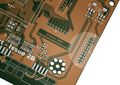
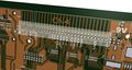
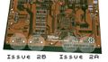
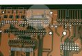
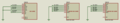
J13 - Daughter board connector - Issue 2A/2B
-
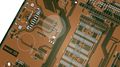 Daughter board location
 -
 Daughter board

J13 - Daughter board connector - Issue 4
-
 J13-I4 daughter location
 -
 J14-I4 circuit daughterboard


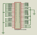
J15 - Next GPIO - Issue 2A/2B
-
 Next GPIO location
 -
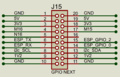 Next GPIO


J15 - Next GPIO - Issue 4
-
 J15-I4 GPIO Location
 -
 J16-I4 Circuit GPIO


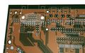
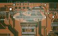
CN5 - Expansion bus (edge connector)
-
 Expansion bus location
 -
 Expansion bus


J10/J11 - Memory Expansion Ports
-
 Mem Expansion location
 -
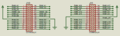 Mem Expanstion

J4/J7 J8/J14 - Joystick Ports
-
 Joystick Ports Location
 -
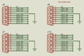 Joystick Ports


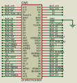
CN1 - VGA Video Port
-
 Video Port Location
 -
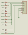 Video Port


Notes:
- In VGA mode (scandoubler enabled), H-SYNC and V-SYNC are carried separately on their respective pins.
- In RGB mode (scandoubler disabled), H-SYNC carries composite sync, and V-SYNC carries 1.
- Pin 14 carries 3V3, which can be connected to SCART pin 16 to indicate RGB to the display.
- There is no convenient source of voltages between 9.5-12V to indicate 4:3 aspect ratio to the display on SCART pin 8, so this is usually left unconnected.
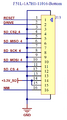
CN8 - Digital Port
-
 Digital Port Location
 -
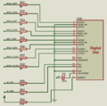 Next Digital Port


CN2/CN6/CN7 - SD Reader (Mainboard) (CN6 on reverse)
-
 SD reader port location
 -
 SD reader main

CN10/CN11/CN12 - SD Reader (Daughterboard) (CN12 on reverse)
-
 SD reader daughter port location
 -
 SD reader

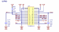
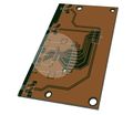
Accelerator Board
-
 Accelerator port location
 -
 Accelerator port


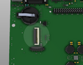
Real Time Clock (RTC)
-
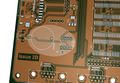 RTC port location
 -
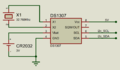 RTC port


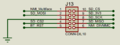
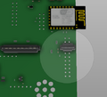
CN9 - ESP8266-01/RS-232 Port
-
 Wifi port location
 -
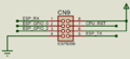 Next ESP port

