Circuit Diagrams: Difference between revisions
From SpecNext Wiki
No edit summary |
No edit summary |
||
| Line 2: | Line 2: | ||
{| width=100% | {| width=100% | ||
|valign=top| [[Image:Circuit_daughter_board_location.jpg]] | |valign=top width=50%| [[Image:Circuit_daughter_board_location.jpg]] | ||
|valign=top| [[Image:Circuit_daughter_board.jpg]] | |valign=top| [[Image:Circuit_daughter_board.jpg]] | ||
|} | |} | ||
| Line 11: | Line 11: | ||
{| width=100% | {| width=100% | ||
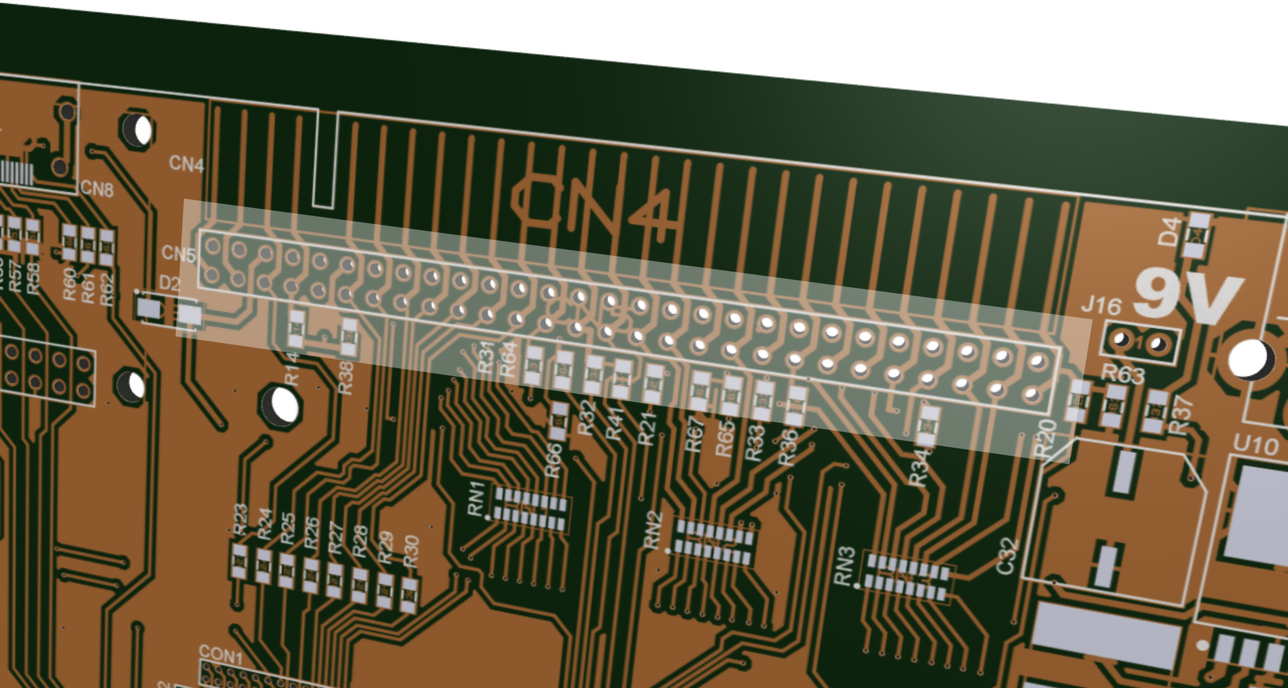
|valign=top| [[Image:Expansion_bus_location.jpg]] | |valign=top width=50%| [[Image:Expansion_bus_location.jpg]] | ||
|valign=top| [[Image:Expansion_bus.jpg]] | |valign=top| [[Image:Expansion_bus.jpg]] | ||
|} | |} | ||
| Line 20: | Line 20: | ||
{| width=100% | {| width=100% | ||
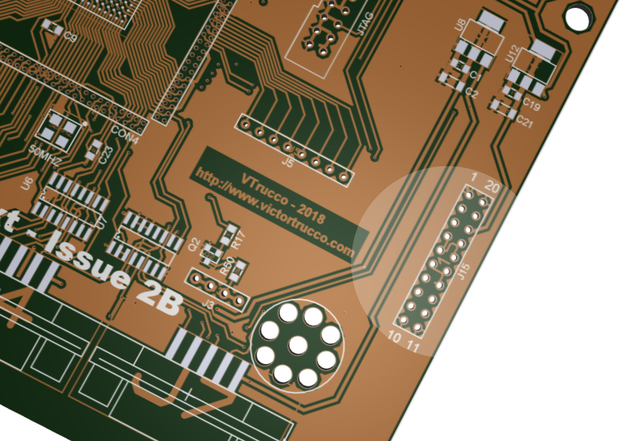
|valign=top| [[Image:NEXT_GPIO_location.jpg]] | |valign=top width=50%| [[Image:NEXT_GPIO_location.jpg]] | ||
|valign=top| [[Image:NEXT_GPIO.jpg]] | |valign=top| [[Image:NEXT_GPIO.jpg]] | ||
|} | |} | ||
<br/> | <br/> | ||
Revision as of 10:54, 20 December 2017
J13 - Daughter board connector
| File:Circuit daughter board location.jpg | File:Circuit daughter board.jpg |
Expansion bus (edge connector)

|
File:Expansion bus.jpg |
Next GPIO

|
File:NEXT GPIO.jpg |