Circuit Diagrams: Difference between revisions
From SpecNext Wiki
No edit summary |
Added link to schematic on gitlab |
||
| Line 1: | Line 1: | ||
== Schematic == | |||
The Issue 2B schematic can be downloaded [https://gitlab.com/thesmog358/tbblue/-/raw/master/docs/schematics/SpecNext.PDF?inline=false here]. | |||
== J13 - Daughter board connector == | == J13 - Daughter board connector == | ||
Revision as of 22:13, 16 February 2020
Schematic
The Issue 2B schematic can be downloaded here.
J13 - Daughter board connector
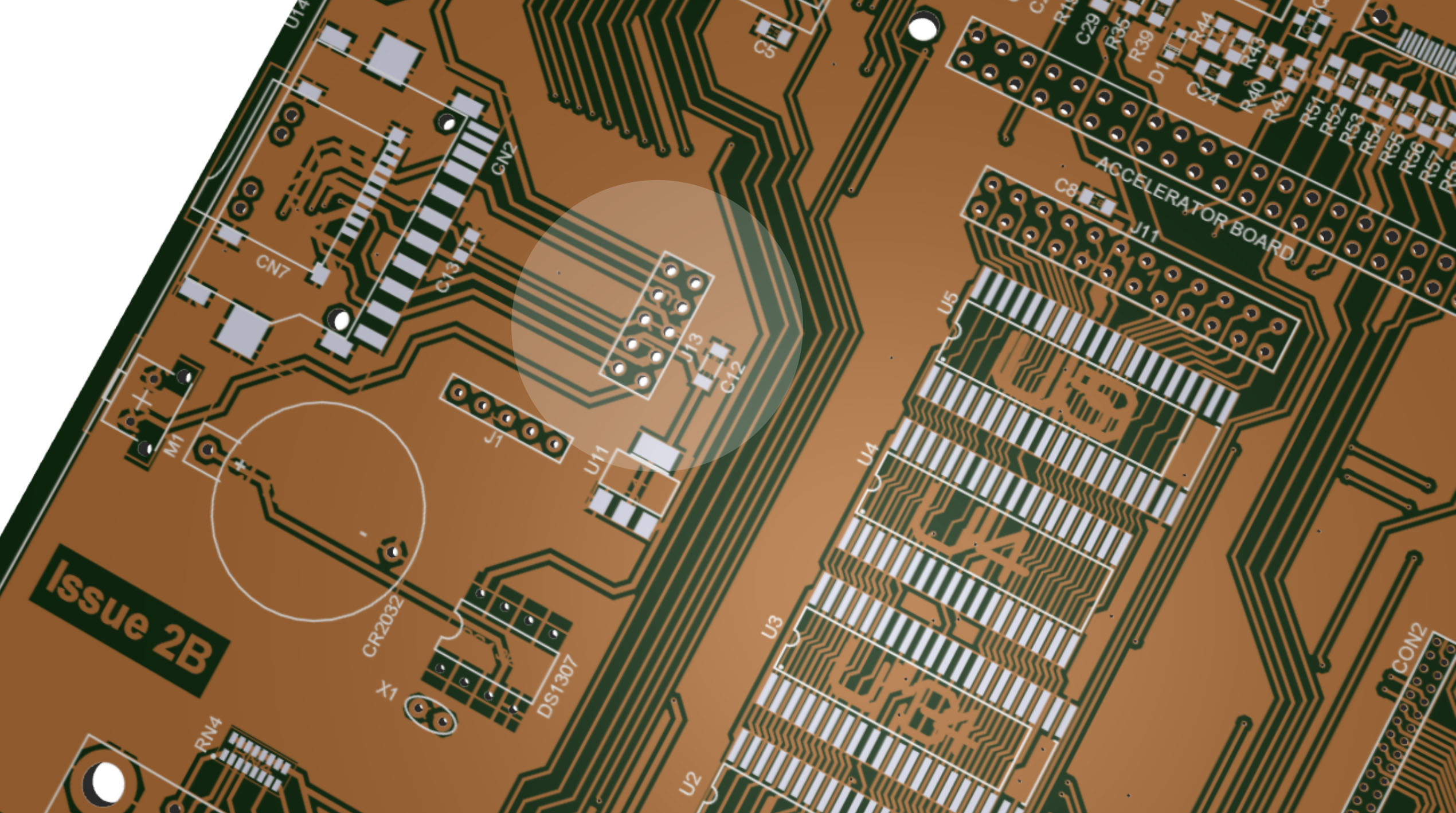
|
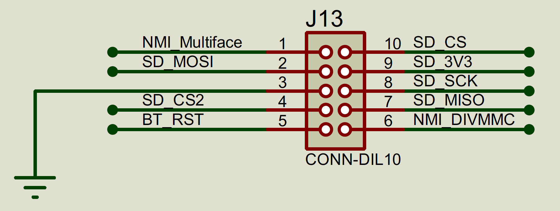
|
J15 - Next GPIO
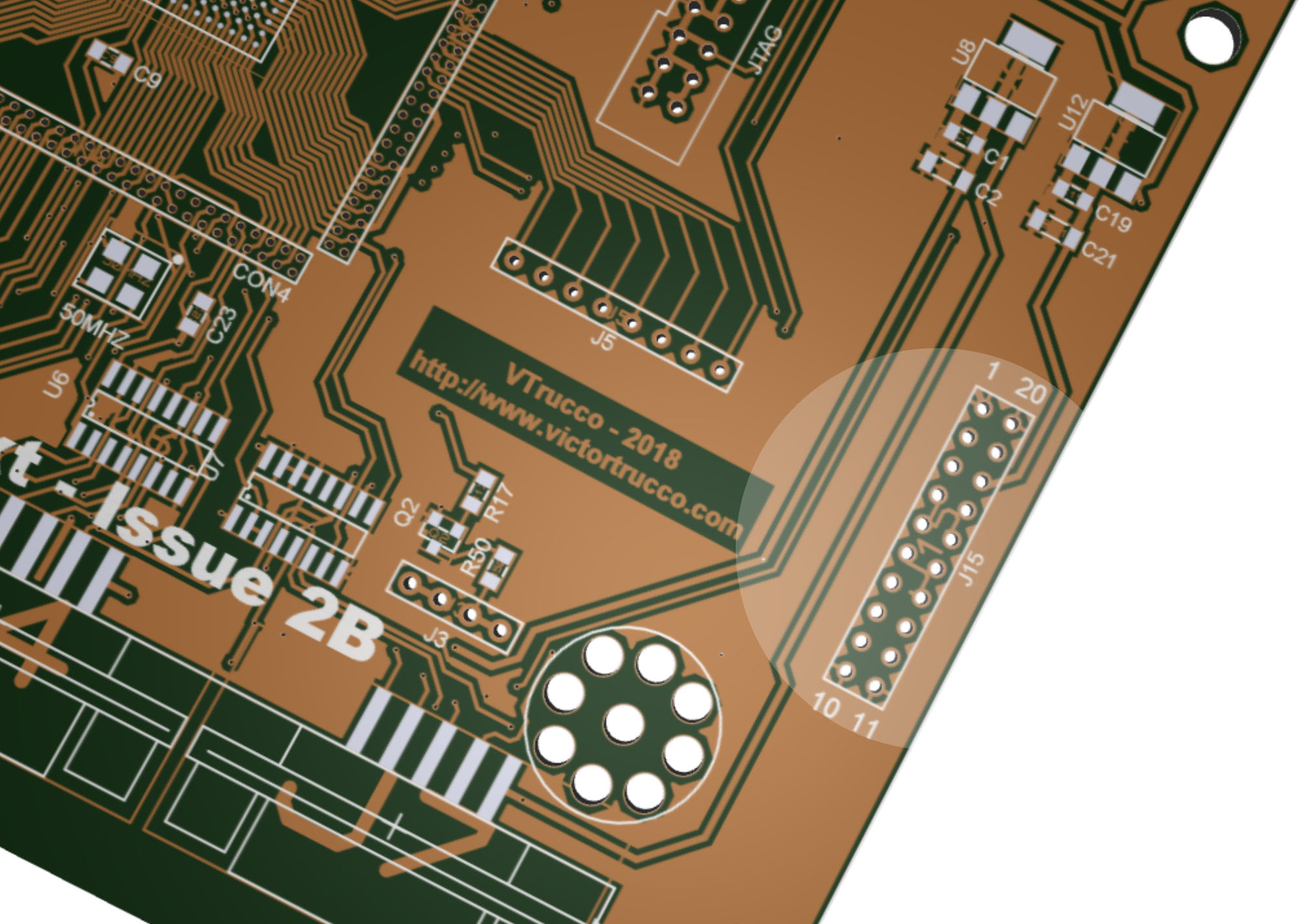
|
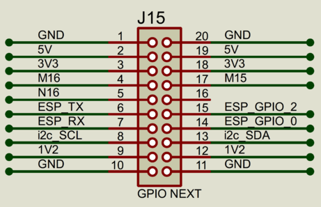
|
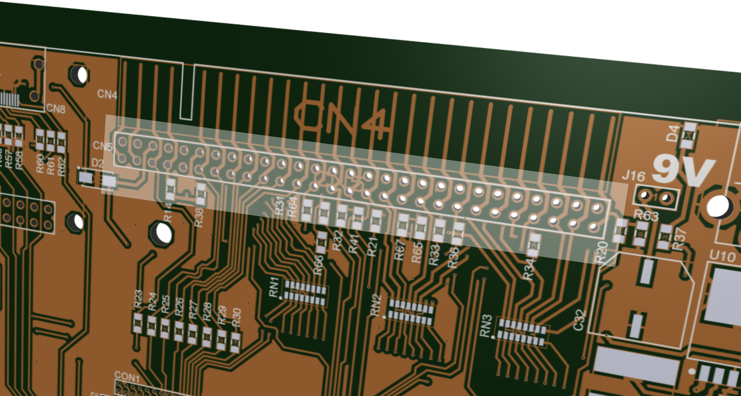
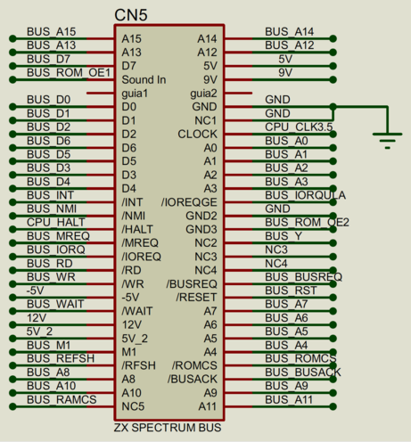
CN5 - Expansion bus (edge connector)
|
|
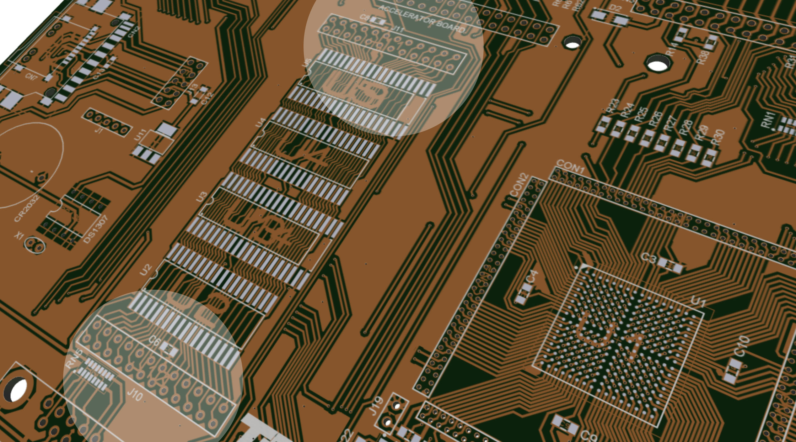
J10/J11 - Memory Expansion Ports
|

|
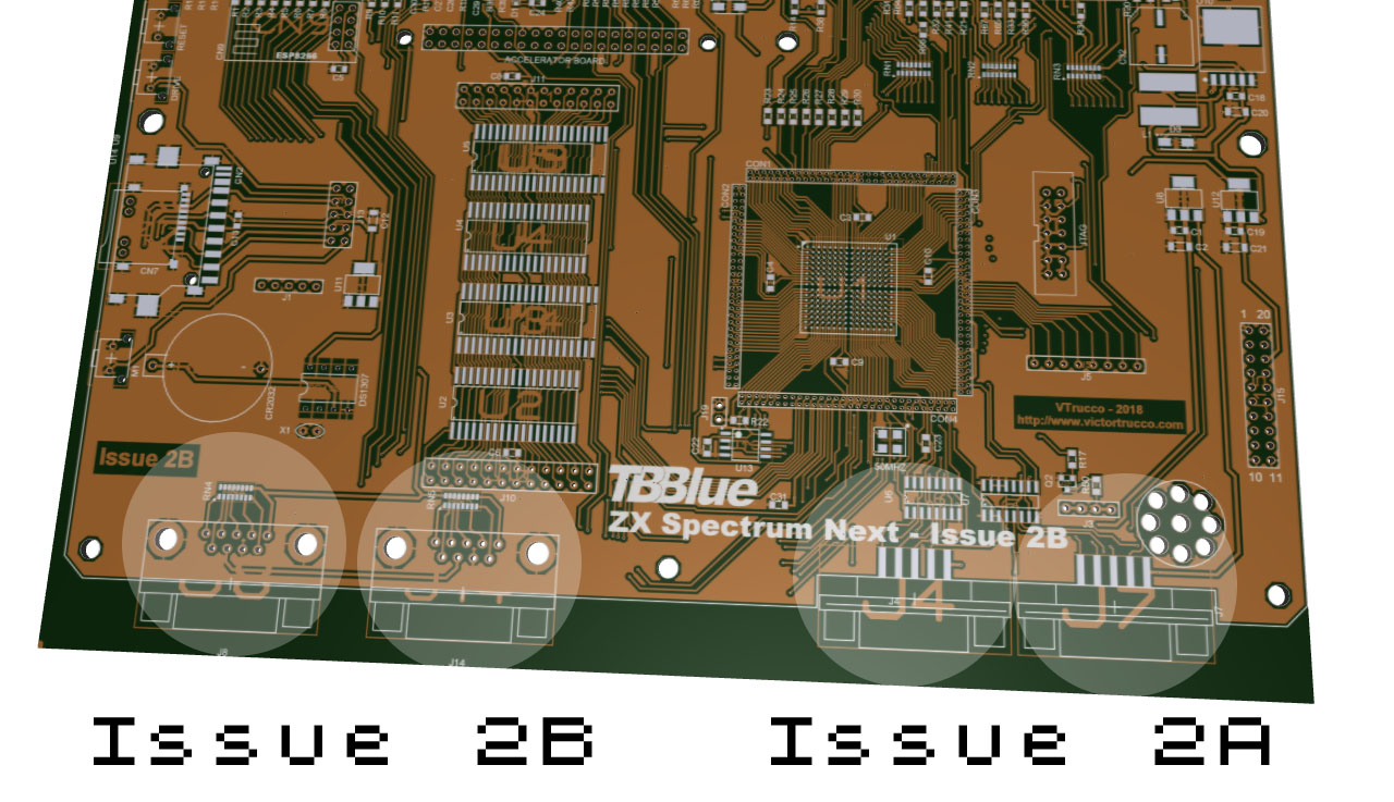
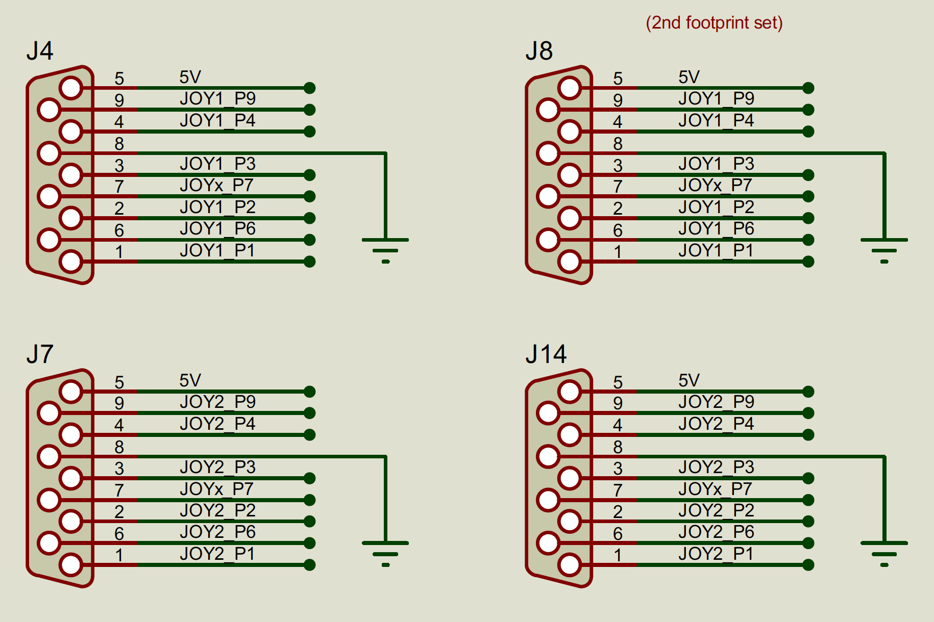
J4/J7 J8/J14 - Joystick Ports
|
|
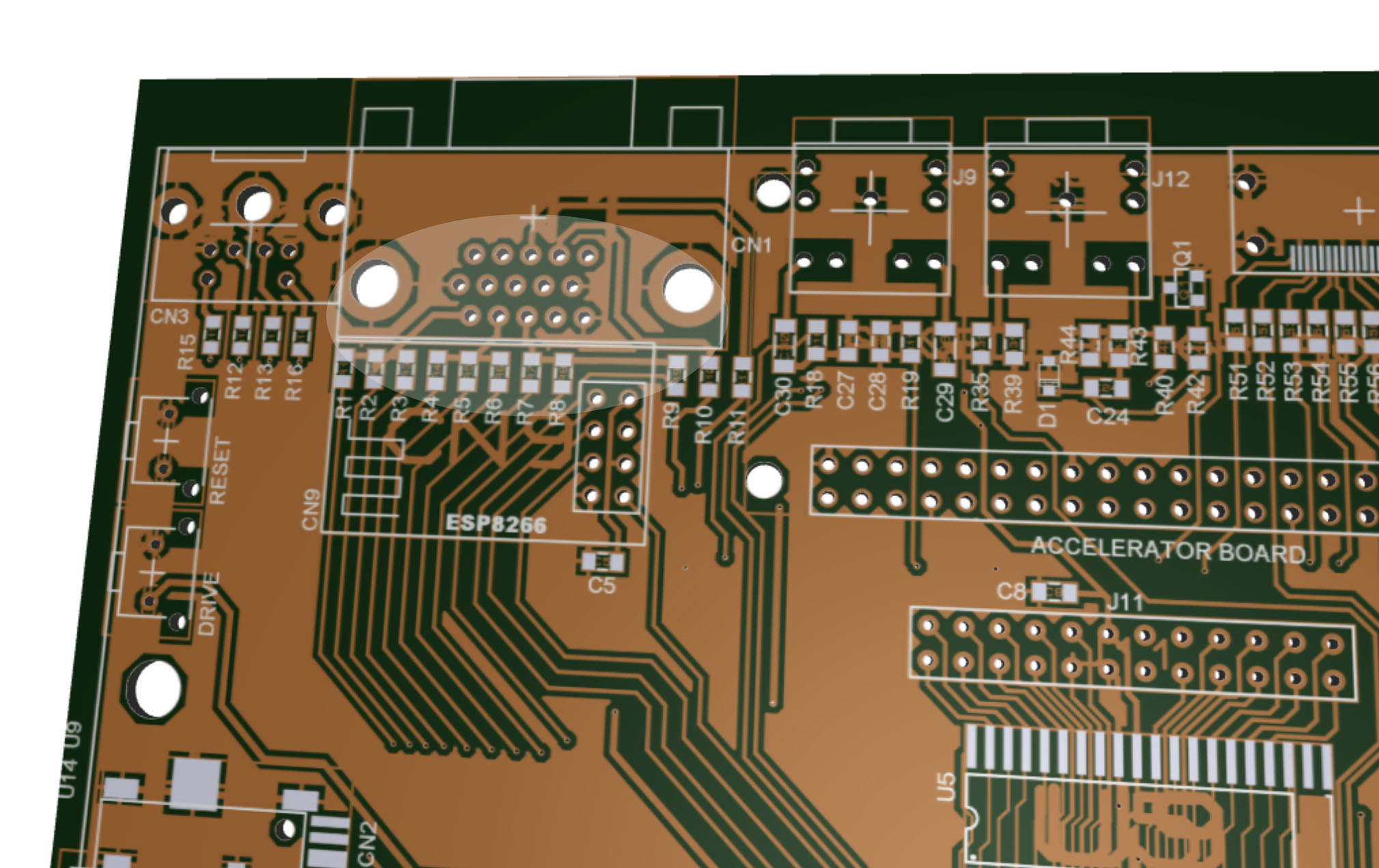
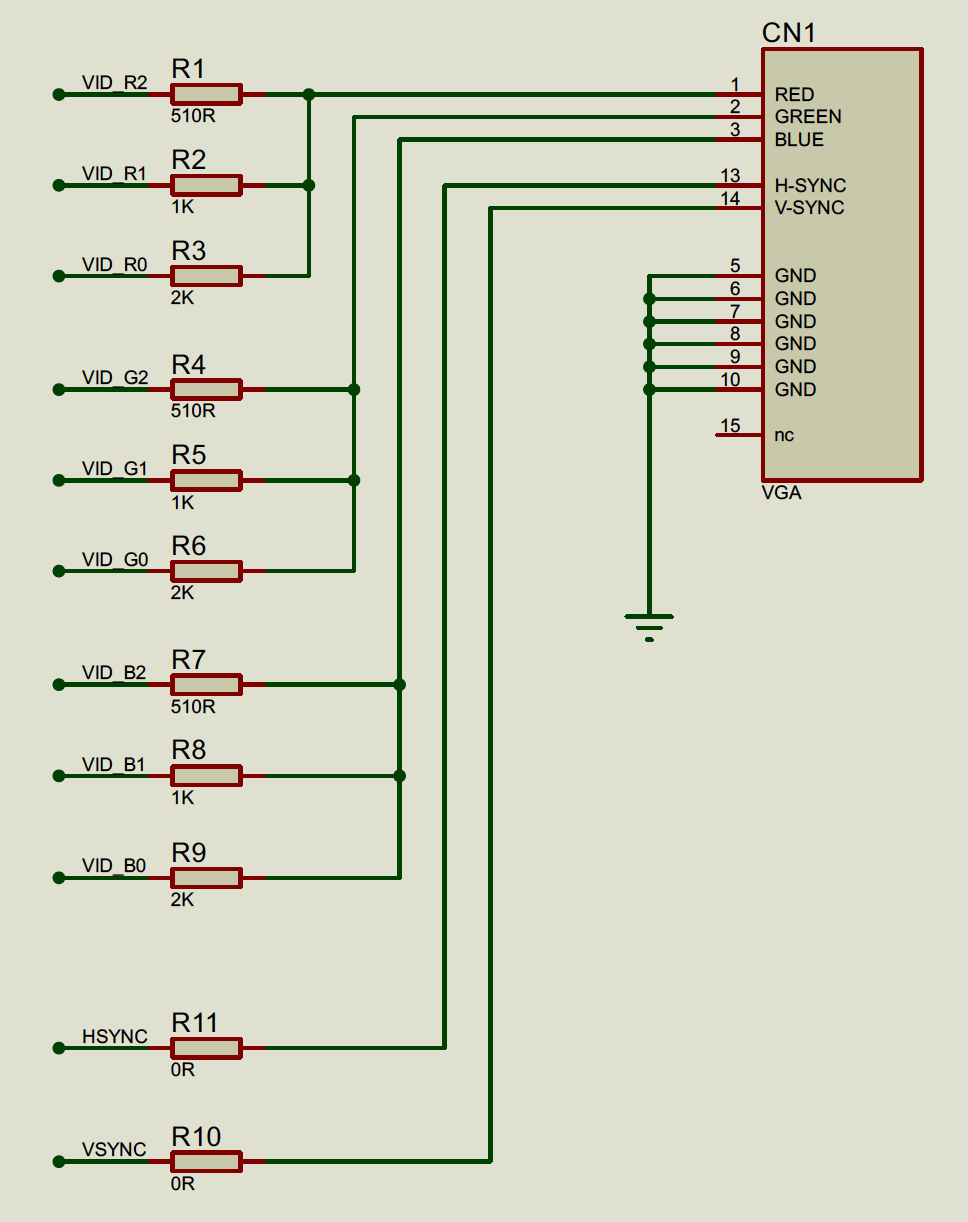
CN1 - VGA Video Port
|
|
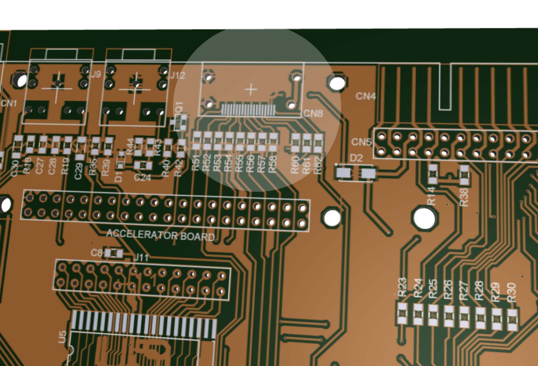
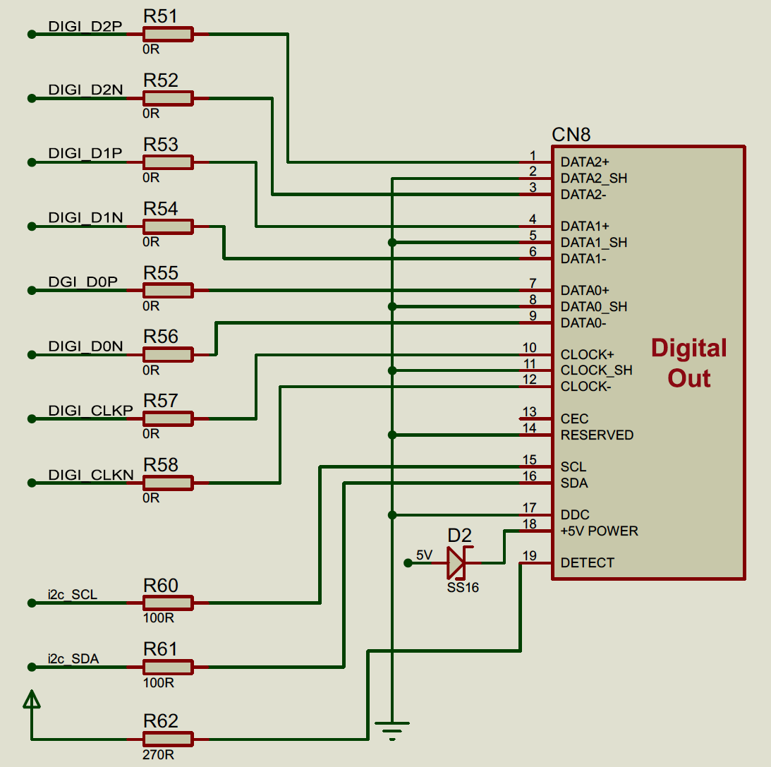
CN8 - Digital Port
|
|
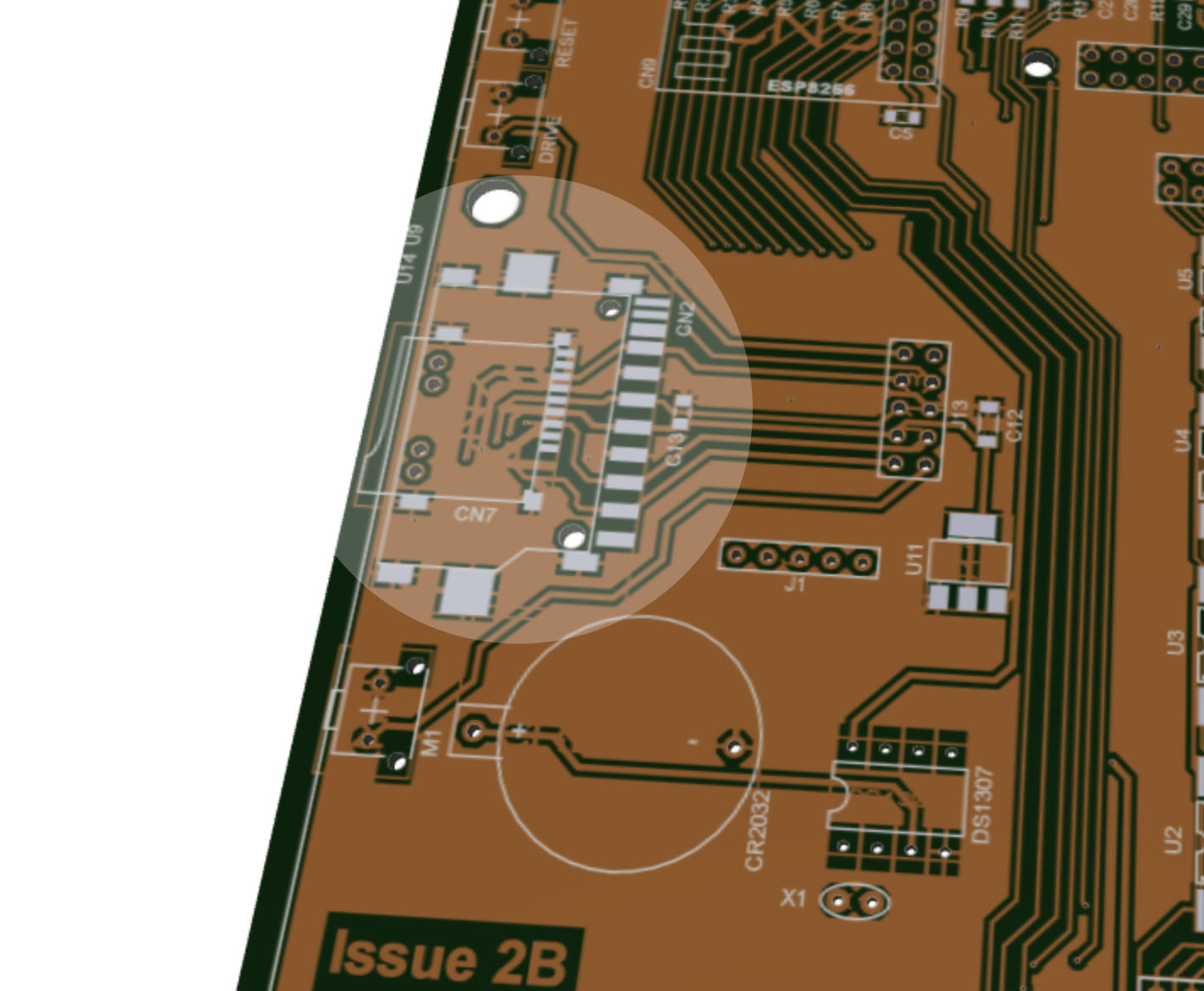
CN2/CN6/CN7 - SD Reader (Mainboard) (CN6 on reverse)
|

|
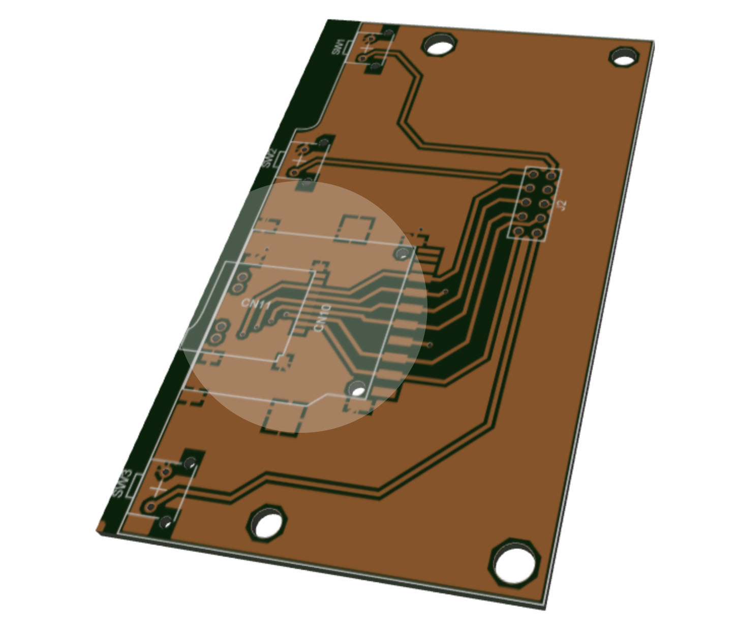
CN10/CN11/CN12 - SD Reader (Daughterboard) (CN12 on reverse)
|

|
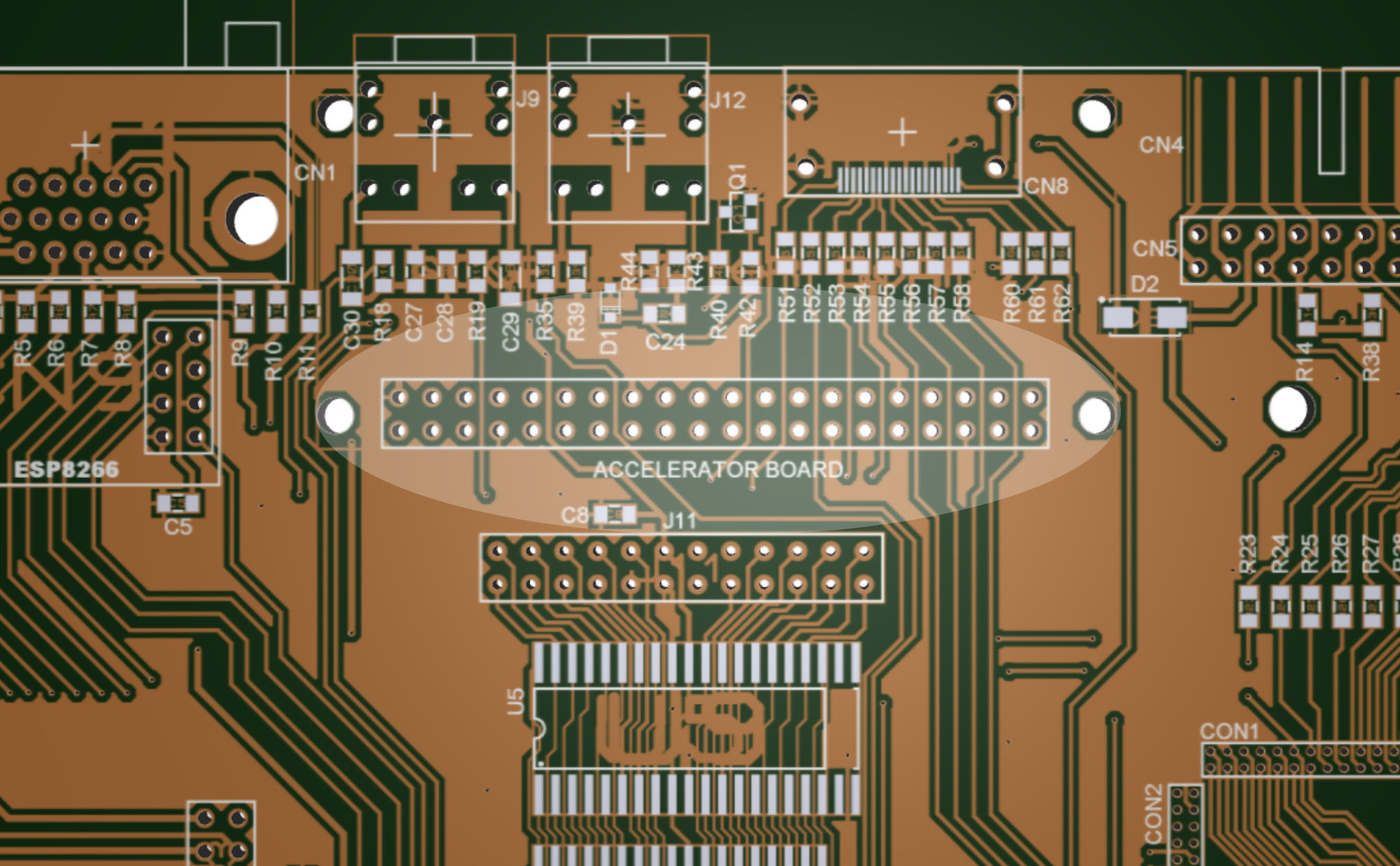
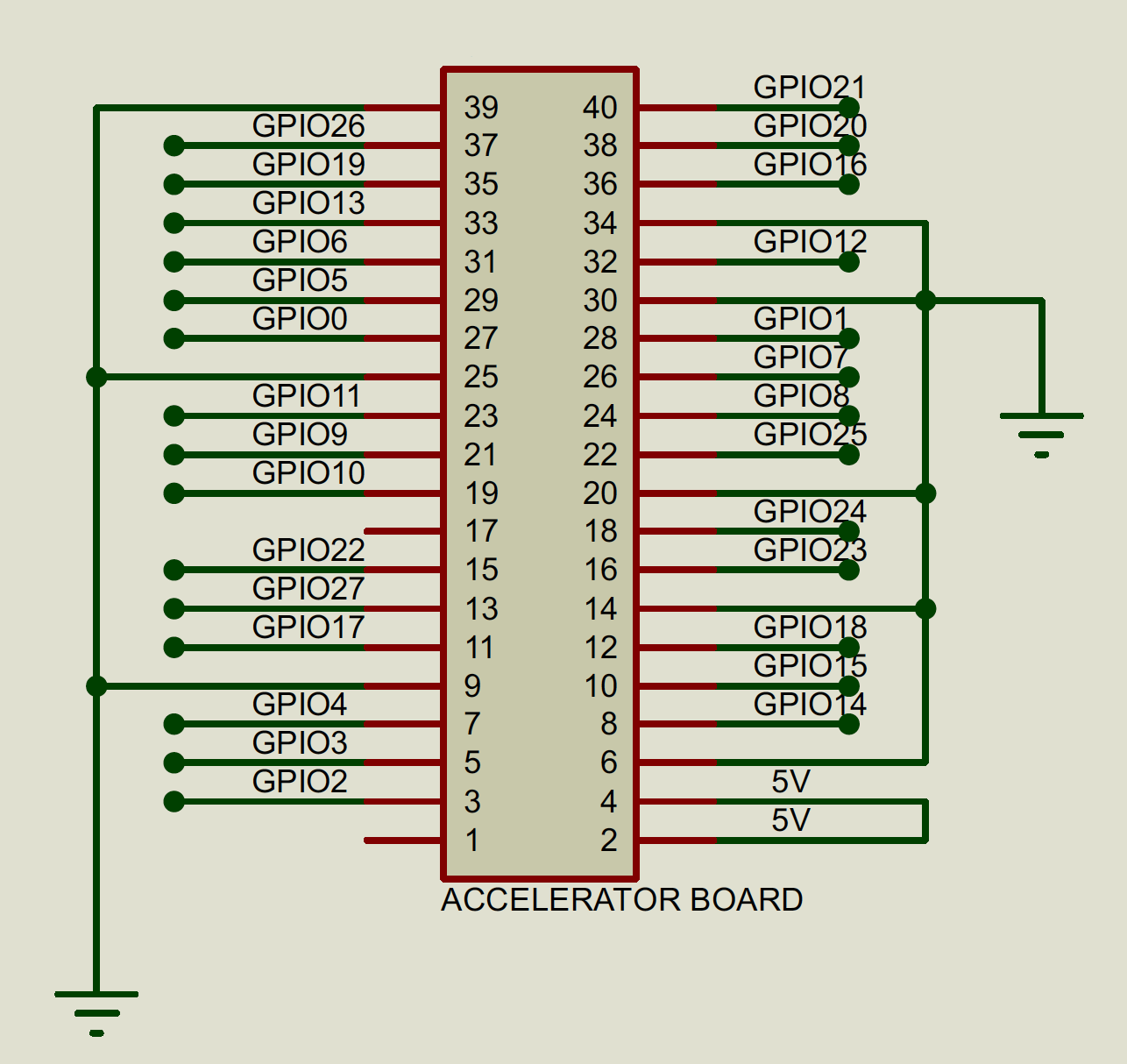
Accelerator Board
|
|
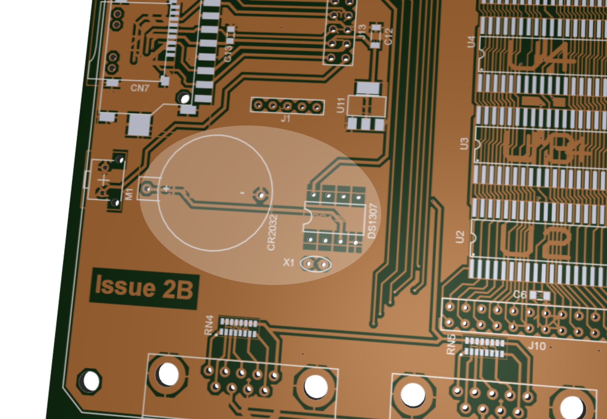
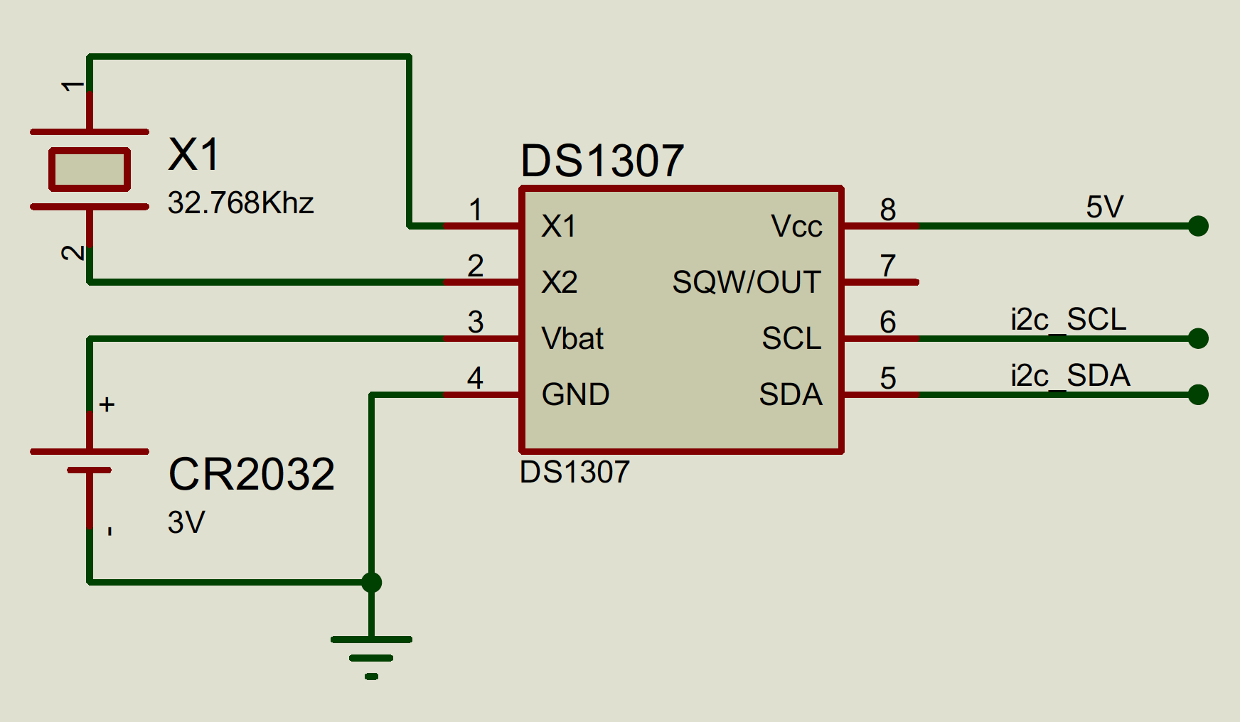
Real Time Clock (RTC)
|
|
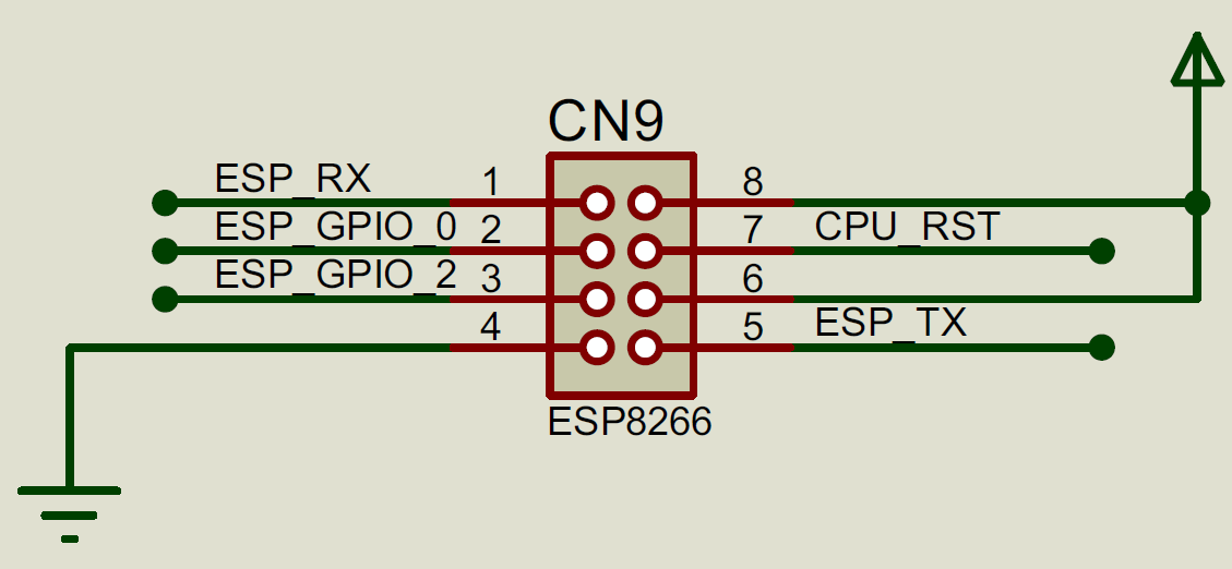
CN9 - ESP8266-01/RS-232 Port

|
|