Circuit Diagrams: Difference between revisions
From SpecNext Wiki
No edit summary |
No edit summary |
||
| Line 3: | Line 3: | ||
{| width=100% | {| width=100% | ||
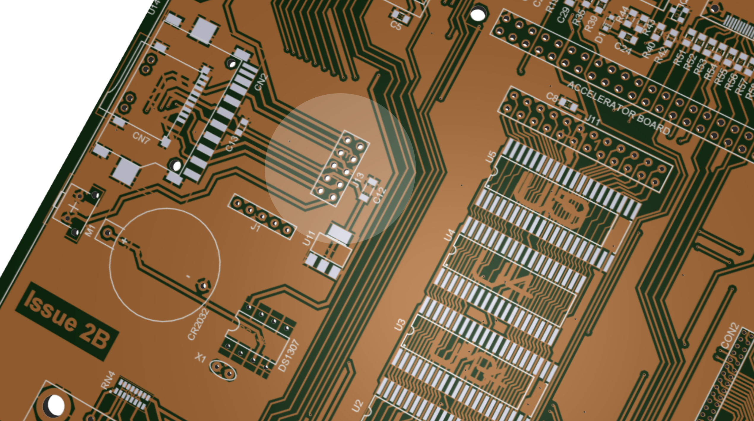
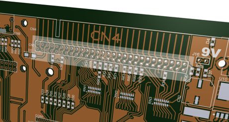
|valign=top width=50%| [[Image:DaughterLocation.jpg | |valign=top width=50%| [[Image:DaughterLocation.jpg]] | ||
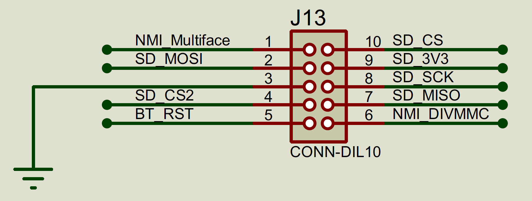
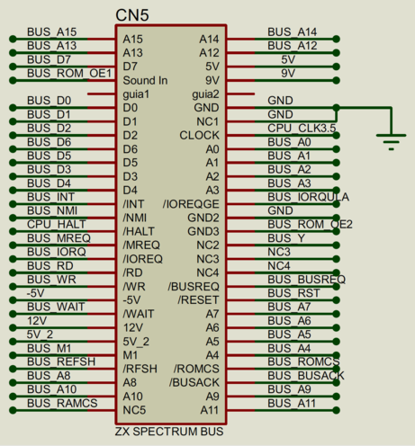
|valign=top| [[Image:Circuit_daughter_board.png | |valign=top| [[Image:Circuit_daughter_board.png]] | ||
|} | |} | ||
